Chinese Academy of Sciences successfully developed terahertz image sensor pixel device
2018-04-16 12:00:10
[China Instrument Network Instrument Development] Liu Liyuan, associate researcher of the High-Speed ​​Image Sensing and Information Processing Task Force of the State Key Laboratory of Superlattices, Institute of Semiconductors, Chinese Academy of Sciences, has developed a pixel device for 860 GHz CMOS terahertz image sensors.
The relevant research results will be published in 2017 in the IEEE Academician Terahertz Science and Technology, a well-known academic journal in the terahertz field.
Terahertz (THz) waves are electromagnetic waves with frequencies between 0.3 THz - 3 THz and wavelengths (1mm ~ 100mm) between millimeter waves and far-infrared light. Terahertz wave imaging technology is emerging as a new type of non-destructive imaging technology. It has very broad application prospects in the fields of biomedicine, medical diagnosis, safety detection, inspection of dangerous goods, detection of stealth weapons, material characterization and flaw detection, and daily use. It has become a hot technology that countries are striving to study.
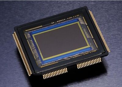
Under the support of the National Key R&D Project, the National Natural Science Foundation of China, the Natural Science Foundation of Beijing, the China Academy of Sciences Youth Innovation Promotion Fund and the Chinese Academy of Sciences Foundation, the research team developed a terahertz pixel device based on standard CMOS technology and its integration. Low-noise signal processing circuit, as shown in Figure 1. The device uses an in-house designed CMOS on-chip antenna, a terahertz band matching network, and a high voltage responsive transistor structure. Under normal temperature operating conditions, the terahertz voltage response rate of the pixel device is 3.3 kV/W @860 GHz, and the noise equivalent power is 106 pW/Hz0.5. The research group also verified the signal processing circuit of the pixel device. It integrates a low-noise chopper instrumentation amplifier and a high-precision SD-ADC, which lays the foundation for monolithic integration of high-resolution terahertz image sensors. Figure 2 shows the experimental results of scanning imaging based on pixel devices.

(a)

(b)
Figure 1 terahertz pixel device structure (a) chip photo (b)

Fig. 2 Imaging results (a) Imaging of leaves (b) Imaging of objects hidden in envelopes
Based on pixel devices, we are expected to further implement large-area array CMOS terahertz image sensors and improve our international competitiveness in the terahertz imaging field.
(Original Title: Semiconductor Institute Develops a Pixel Device for 860-GHz CMOS Terahertz Image Sensors)